Failure analysis is an important part of the reliability work of electronic assembly process, and it is necessary to have certain testing and analysis equipment to carry out failure analysis of electronic process. Failure analysis includes investigation and analysis of failure conditions, identification of failure modes, description of failure characteristics, assumption and determination of failure modes, and proposals for corrective measures and prevention of new failures.
The failure analysis of the electronic assembly process is to check and analyze the failure phenomena related to the assembly process of the solder joints, vias, and wirings that are judged to be invalid according to the performance failure. The purpose is to discover and determine the failure causes and mechanisms related to the assembly process, then to feed back to the design, manufacture and user to prevent recurrence of failure and improve the process reliability of electronic products. The functions are as below:
(1) To improve the method of hardware design, process design and reliability application.
(2) To find out the physical phenomenon that causes failure, and obtain a model for reliability prediction.
(3) To provide theoretical basis and practical analysis means for reliability test (accelerated life and screening test) conditions.
(4) During processing, to determine whether it is a batch problem, and provide a basis for whether batch recall and scrapping are required.
(5) To improve product yield and reliability through failure analysis and corrective measures, reduce product operation failures, and obtain certain economic benefits.
Electronic assembly process failure analysis techniques mainly include: appearance inspection, metallographic section analysis, optical microscope analysis technology, infrared microscope analysis technology, acoustic microscope analysis technology, scanning electron microscope technology, electron beam testing technology, x-ray analysis technology and staining and penetration analysis techniques. This chapter will focus on the principles and methods often used in failure analysis.
1. Visual inspection
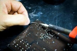
Appearance inspection is mainly to analyze appearance defects, the purpose is to record the physical dimensions, materials, design, structure and marks of PCB, components and solder joints, confirm the damage of appearance, detect pollution and other abnormalities and defects, these problems are all process manufacturing or application evidence of errors, overloads, and operational errors caused by the device are likely to be relevant to the failure. Visual is usually used for appearance inspection, and 1.5-10 times magnifying glass or optical microscope can also be used. Appearance inspection should pay special attention to the following aspects:
(1) Mechanical damage
(2) Device sealing defects
(3) Plating defects of device pins
(4) Pollution or adhesion on the surface of the PCB
(5) Delamination and bursting of PCB, etc.
(6) Thermal damage or electrical damage to the device
(7) Abnormal surface treatment of PCB pads
- Solder joint defects
2. Metallographic section analysis
Metallographic analysis is an important means of experimental research on metal materials. Quantitative metallographic principles are used to determine the three-dimensional spatial morphology of the alloy structure by measuring and calculating the metallographic microstructure of the two-dimensional metallographic sample grinding surface or thin film, so as to establish quantitative relationship between alloy composition, structure and properties.
Metallographic sample preparation process is:
(1) Determination of sample selection location and interception method: select the sampling location and inspection surface. This process comprehensively considers the characteristics of the sample and the processing technology, and the selected location must be representative.
(2) Mounting: Take a special mold for metallographic section, place the sample upright in the mold, and let the part to be inspected face up. Take a paper cup and mix cold embedding resin (solid state) and curing agent (liquid state) at a volume ratio of 2:1, stir evenly, pour into the mold until the sample is completely submerged, and let the mold stand for 10-20 minutes until the resin is completely cured.
(3) Sample coarse grinding: The purpose of coarse grinding is to flatten the sample and grind it into a suitable shape. After the solidification is complete, firstly grind the sample with coarser metallographic sandpaper until it is close to the part to be inspected, then perform coarse grinding and fine grinding according to the order of metallographic special sandpaper mesh from small to large.
(4) Sample fine grinding: The purpose of fine grinding is to eliminate the deep scratches left by rough grinding and prepare for polishing. For general material grinding methods are divided into manual grinding and mechanical grinding.
(5) Sample polishing: The purpose of polishing is to remove the fine grinding marks left by the polishing and become a bright and traceless mirror surface. It is generally divided into three types: mechanical polishing, chemical polishing, and electrolytic polishing, and the most commonly used is mechanical polishing. Polishing powder particle size is about 0.05um
(6) Sample micro-etching: The microscopically observed tissue of the polished sample must undergo metallographic corrosion. There are many methods of corrosion, mainly chemical corrosion, electrolytic corrosion, constant potential corrosion, and the most commonly used is chemical corrosion, the micro-etching solution is mixed with concentrated ammonia water and 30% hydrogen peroxide in a volume ratio of 9:1) to be tested The surface is smeared for about 10 seconds, then the surface is cleaned with clean water and dried.
(7) Observation: According to the specific conditions of the part to be inspected, select an appropriate magnification until the real image can be clearly observed.
3. Analytical technology
X-ray analysis technology is a high technology that uses X-rays to identify atomic species. X-rays are short-wavelength, high-energy electromagnetic waves. When X-rays are used to irradiate a substance, in addition to scattering and absorption, it will also cause ionization of the electrons in the atom, and the electrons in the inner orbit will leave the atom to form a vacancy, making the atom in an “excited state”, so that the outer electrons It will automatically jump to the inner layer to fill the gap, thus emitting X-rays with a certain energy. Because its wavelength and energy are different from those of the original X-rays, it is called secondary X-rays, also known as X-ray fluorescence.
The X-ray transmission system is to use different material thicknesses or different material densities to image different principles of X-ray absorption or transmittance, and is used to check internal defects in solder joints, internal defects in through holes, and high-density packaged BGA or CSP devices. Locating defective solder joints, and checking PCB internal defects, etc. X-ray analysis is a non-destructive testing analysis technique.
4. Optical microscope analysis technology
Optical microscope is one of the main tools for failure analysis of electronic components, semiconductor devices and integrated circuits. There are mainly stereo microscopes and metallographic microscopes. The combination of the two can be used to observe the appearance of the device and the surface shape, distribution, size, structure, structure, defect and stress of the failure site, such as observing and analyzing various burnout and breakdown phenomena of the chip under overelectric stress, Internal and external bonding of leads, chip cracks, contamination, scratches, oxide layer defects, and metal layer corrosion.
The magnification of the stereo microscope is low, from several times to hundreds of times, but the depth of field is large. The magnification of the metallographic microscope is high, ranging from tens of times to more than one thousand times, but the depth of field is small. Except for the difference in magnification, the structures, imaging principles and methods of use of the two are basically similar. Both use the combination of eyepiece and objective lens to form an image. The stereoscopic microscope is generally called the positive image, and the image formed by the metallographic microscope is the inverted image. The magnification of the image is the product of the magnifications of the eyepiece and the objective. Stereo microscopes and metallographic microscopes have two types of photography, incident and transmission, and are equipped with some auxiliary devices, which can provide observation methods such as bright field, dark field, differential interference contrast and polarization to meet the needs of different observations.
5. Acoustic microscope analysis technology
Acoustic microscope: scanning Acoustic Microscope, has become one of the fastest-growing technologies in non-destructive testing technology, mainly for failure analysis of semiconductor devices, chips, and materials. It can check: 1. The lattice structure and impurity particles inside the material, inclusions, precipitate etc. 2. Internal cracks. 3. Delamination defects. 4. Voids, bubbles, voids, etc.
It mainly includes three kinds of acoustic microscopes: scanning laser acoustic microscope (SLAM), scanning acoustic microscope (SAM) and C-Mode Scanning Acoustic Microscope (C-SAM). In terms of depth, each type of acoustic microscope uses its own application area. For example, SLAM can observe all areas inside the sample, C-SAM can observe the area a few millimeters below the surface of the sample, and SAM can only observe the sample surface area of a few microns.
C-SAM is a reflective scanning acoustic microscope, which is an important technology in nondestructive testing technology. It uses the amplitude, phase and polarity changes generated by the reflection of high-frequency ultrasonic waves on the discontinuous interface of the material to image, and its scanning method is to scan the information of the X-Y plane along the Z-axis. The principle of internal imaging is that the electric energy generates ultrasonic waves through the focusing conversion mirror and strikes the object to be tested. The sound waves are reflected or penetrated on different interfaces, and the signals are received. After image processing, the images and signals are analyzed.
C-SAM makes the most use of this characteristic to detect the defects inside the material and image them according to the change of the received signal. Therefore, as long as there are defects such as delamination, air holes, cracks, etc. on the surface of the detected IC or the interface of the internal chip construction material, the relative position of the defect can be known from the C-SAM image.
At present, the C-mode ultrasonic scanning acoustic microscope is mainly used for electronic packaging or assembly analysis. A typical scanning acoustic image is a red warning color to indicate the existence of defects.
Due to the application of a large number of plastic-encapsulated components in the SMT process, in the process of converting the lead-based process to the lead-free process, due to the moisture sensitivity of the device, the wet plastic-encapsulated device is prone to internal delamination cracking phenomenon. PCB boards are also prone to board explosion. At this time, the scanning acoustic microscope highlights its advantages in non-destructive flaw detection analysis technology.


